FEI Helios NanoLab 650
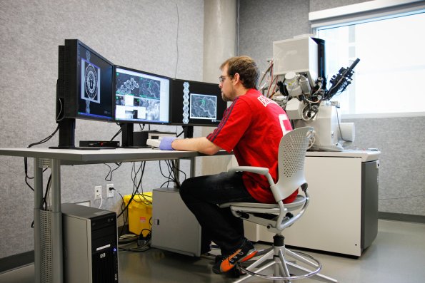
FEI Helios 650 dbFIB
The Focused Ion Beam Dual Beam Microscope is a scanning microscope with very high-resolution topographical imaging and etching capabilities. The Helios NanoLabTM 650 features FEI’s most recent advances in field emission SEM (FESEM) and focused ion beam (FIB) technologies and their combined use. It is designed to access a new world of extreme high resolution (XHR) 2D and 3D characterization, nanoprototyping, and higher quality sample preparation.

When publishing work with data collected from the dbFIB, the following should be used for acknowledgment:
“This work made use of University of Utah USTAR shared facilities support, in part, by the MRSEC Program of NSF under Award No. DMR-1121252.”
Instrument Features
• Best-in-class Elstar™ monochromated Schottky FESEM technology and performance, with subnanometer resolution from 1 to 30 kV
• FEI’s exclusive Tomahawk FIB, featuring excellent imaging, outstanding low kV operation down to 500 V and up to 65 nA beam current
• Differential pumping and TOF correction for higher resolution ion beam imaging, milling and deposition
• 150 x 150 mm high precision, high stability piezo stage
• Unique imaging technologies and solutions, including generation II of Helios advanced detectors, process monitoring, FEI SmartSCAN™ and DCFI to help imaging charging samples
• Most complete and integrated suite of prototyping capabilities, with 16-bit pattern generator for FIB & SEM, advanced patterning features library, and largest beam chemistry selection and expertise
• Best-in-class thin sample preparation and 3D characterization and analysis
• Most advanced process monitoring and endpointing capabilities
Elstar XHR immersion lens FESEM column
• Elstar electron gun with:
– Schottky thermal field emitter
– Hot-swap capability
– UC technology (monochromator)
• 60 degree dual objective lens with pole piece protection
• Heated objective apertures
• Electrostatic scanning
• ConstantPower™ lens technology
• Beam deceleration with stage bias from -50 V to -4 kV
• Integrated Fast Beam Blanker*
Tomahawk ion column
• Superior high current performance, with up to 65 nA max beam current
• Lowest voltage (500 V) for ultimate sample preparation quality
• 2-stage differential pumping
• Time-of-flight (TOF) correction
• 15 apertures
Detectors:
• Elstar in-lens SE detector (TLD-SE)
• Elstar in-lens BSE detector (TLD-BSE)
• Everhart-Thornley SE detector (ETD)
• IR camera for viewing sample/column
• High performance SE and SI (secondary ion) detector (ICE)*
• Retractable low voltage, high contrast solid-state electron detector (DBS)*
• NavCam – CCD Camera for sample navigation
• Energy Dispersive Spectroscopy (element ID and semi-quantitative analysis) EDAX
• Electron Backscatter Diffraction (grain analysis and crystal orientation) EDAX
Sample size
• Maximum size: 150 mm diameter with full rotation (larger samples possible with limited rotation)
• Maximum clearance between stage and coincidence point: 55 mm
• Weight: max. 500 g (including the sample holder)
Sample holders
• High-resolution multi-stub mount holder
• Vise Specimen Holder to clamp irregular, large or heavy specimens to the specimen stage*
• Universal Mounting Base (UMB) for stable, flexible mounting of many combinations of samples and holders such as flat and pretilt stubs, and row holders for TEM grids*
• Various wafer and custom holder(s) available by request*
dbFIB Features and Applications
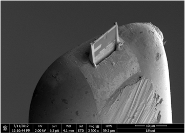
• Slice-n-view: the ability to incrementally image then cut 10 nm slices into the face of a 5um X 5um area, then rebuilding the images into a tomographic volume.
• Deposit Pt in pre-defined patterns, down to ~35 nm line widths
• Mill patterns using the FIB as a precision scalpel
Create precision cross-sections for in-situ viewing
• Selectively remove organic material by precision FIB cutting, using injected water vapor enhanced etching
• UHR- SEM column: with sub nm resolution
• Omniprobe tool, gives the ability to prepare samples for TEM analysis
Selected Publications
1. Zhang, Y., Edwards, M.A., German, S.R., and White H.S., Multipass Resistive-Pulse Observations of the Rotational Tumbling of Individual Nanorods, J. Phys. Chem, C., 2016, Article ASAP, DOI: 10.1021/acs.jpcc.6b02018.
2. Xiong, J., Chen, Q., Edwards, M.A., and White, H.S., Ion Transport within High Electric Fields in Nanogap Electrochemical Cells, ACS Nano, 2015, 9, 8520 – 8529.
3. Edwards, M.A., German, S.R., Dick, J.E., Bard, A.J., and White, H.S., High-Speed Multipass Coulter Counter with Ultrahigh Resolution, ACS Nano, 2015, 9, 12274 – 12282.
Hourly Rate
In-State Academic Users: $ 50.00
Out of State Academic Users: $ 75.50
Industry Rate: $ 100.00
Automated Overnight Run Rate (5:00pm – 8:00am)
In-State Academic Users: $ 200.00
Out of State Academic Users: $ 302.00
Industry Rate: $ 400.00
For tech support rates see please see our complete billing rates.